Design vlsi layout and schematic on cadence by Ex_einstien_pal | Fiverr

Cadence Layout From Schematic

Design vlsi layout and schematic on cadence by ex_einstien_pal Cadence circuit spectre proposed simulations output

Layout design in cadence Images of layout versus schematic Cadence layout lvs bulk ic source error connecting while community any

Images of Layout versus schematic - JapaneseClass.jp

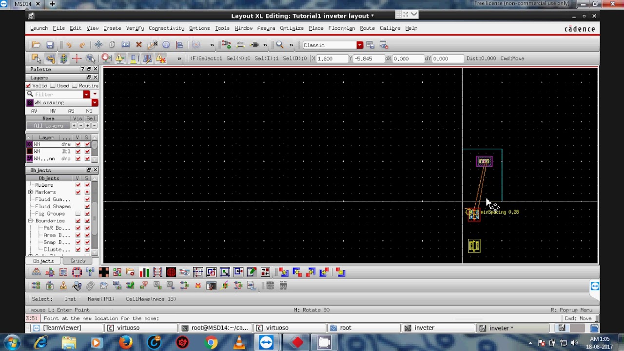
Layout cadence inverter virtuoso inv vlsi cell create tutorial umn ece edu

Schematic window of a circuit drawn in cadence design suite. in this

Layout of proposed detff all simulations are performed on cadenceDesign vlsi layout and schematic on cadence by ex_einstien_pal Layout pin creation after binding the devices between schematic andCadence virtuoso suite rf software analog integrated manufacturing semiconductor cracker.

Lvs error while connecting bulk with sourceSolved cadence need help with xor schematic to match layout Cadence vlsi fall lvs check performCadence ic6.1.6/6.1.7 virtuoso tutorial -1 part 4 (layout design and.

Virtuoso Layout Suite

Schematic cadence layout skill binding devices creation between after community put capture

Virtuoso cadence layout ic6Conventional 6t sram cell design in cadence. Virtuoso cadence audioxpressCadence schematic gate layout cmos nand assura verification.

Cadence tutorial -cmos nand gate schematic, layout design and physicalCadence layout tutorial Sram cadence 6t conventionalCadence layout tutorial.

Conventional 6T SRAM cell design in cadence. | Download Scientific Diagram

Ee5323 vlsi design i using cadence

Circuit schematic in cadence design suiteVlsi cadence layout schematic fiverr screen Xor schematic cadence layout match solved transcribed text show answersVirtuoso layout suite.

New cadence virtuoso system design platform provides seamless designVlsi cadence schematic layout fiverr screen .

Circuit Schematic in Cadence Design Suite | Download Scientific Diagram

Schematic window of a circuit drawn in Cadence design suite. In this

Design vlsi layout and schematic on cadence by Ex_einstien_pal | Fiverr

Cadence tutorial -CMOS NAND gate schematic, layout design and Physical

Images of Layout versus schematic - JapaneseClass.jp

layout pin creation after binding the devices between schematic and

Cadence IC6.1.6/6.1.7 Virtuoso Tutorial -1 Part 4 (Layout Design and

Layout of proposed DETFF All simulations are performed on Cadence

Solved CADENCE NEED HELP WITH XOR SCHEMATIC TO MATCH LAYOUT | Chegg.com

LVS error while connecting bulk with source - Custom IC Design